Questions on Semiconductors and the p-n Junction, the kind your examinations ask. Solve one on paper. Then tell the book how it went. The book believes you, and it uses your answer to plan your revision.
0%
Nothing marked yetMark honestly. Peek at the answer only after your own attempt.
Energy Bands, Doping and the p-n Junction
24 questions · after Lesson 4, Forward and Reverse Bias: the Diode Curve
Energy bands
Q1
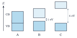
The figure shows the valence band (VB) and conduction band (CB) of three solids A, B and C.
Which is a metal, which a semiconductor and which an insulator? Give the reason for each.
In which solid are there free electrons even at \(0\) K?
Answer(i) A metal, B semiconductor, C insulator (ii) A
Solution
A: the bands overlap, so electrons move freely into empty states. A metal. B: a gap of about \(1\) eV, small enough for thermal energy to lift some electrons across. A semiconductor. C: a gap of \(6\) eV, far too large. An insulator.
Only A. In B and C every electron is in the full valence band at \(0\) K and nothing can move.
How did it go?
Q2
The band gaps are: silicon \(1.1\) eV, germanium \(0.7\) eV, diamond \(5.5\) eV. Take \(hc = 1240\) eV nm.
Find the longest wavelength of light that can lift an electron across each gap.
Which of the three absorb visible light (\(400\) to \(700\) nm)? Why is diamond transparent?
Answer(i) \(1130\), \(1770\), \(225\) nm (ii) Si, Ge
Visible photons carry \(1.8\) to \(3.1\) eV. This is more than the gaps of Si and Ge, so both absorb visible light and look dark. It is far less than \(5.5\) eV, so diamond cannot absorb it; the light passes through.
How did it go?
Q3
When the temperature rises, the resistance of a metal increases but that of a semiconductor decreases. Explain both.
Answermetal: more scattering; semiconductor: more carriers
Solution
Metal: the number of free electrons is fixed. Heating makes the ions vibrate more, the electrons are scattered more often, and the resistance rises.
Semiconductor: heating lifts many more electrons across the gap, creating electron-hole pairs. The number of carriers grows very fast with temperature. This outweighs the extra scattering, so the resistance falls.
How did it go?
Q4
Pure silicon has \(5 \times 10^{28}\) atoms per m\(^3\). At \(300\) K it has \(n_i = 1.5 \times 10^{16}\) free electrons per m\(^3\).
How many holes per m\(^3\) are there? Why?
What fraction of the atoms has lost an electron to the conduction band?
Answer(i) \(1.5 \times 10^{16}\) (ii) \(3 \times 10^{-13}\)
Solution
\(1.5 \times 10^{16}\) per m\(^3\). Every electron that leaves the valence band leaves one hole behind, so in a pure crystal \(n_h = n_e = n_i\).
\(\dfrac{1.5 \times 10^{16}}{5 \times 10^{28}} = 3 \times 10^{-13}\). About one atom in three million million. Pure silicon is a very poor conductor.
How did it go?
Q5
What is a hole? How does a hole "move" when an electric field is applied, and what is its effective charge?
Answerempty bond state; electrons hop in; \(+e\)
Solution
A hole is a missing electron in a covalent bond of the valence band, an empty state where an electron should be.
Under a field a neighbouring bound electron jumps into the hole, leaving a new hole where it came from. The empty state moves the opposite way to the electrons, so it behaves like a free particle of charge \(+e\).
How did it go?
Q6
The conductivity is \(\sigma = e(n_e\mu_e + n_h\mu_h)\). For pure silicon \(\mu_e = 0.135\) m\(^2\)/V s and \(\mu_h = 0.048\) m\(^2\)/V s. Take \(e = 1.6 \times 10^{-19}\) C and \(n_i\) from Question 4. Find \(\sigma\) and the resistivity.
Answer\(4.4 \times 10^{-4}\) S/m, \(2.3 \times 10^{3}\ \Omega\) m
Resistivity \(\rho = \dfrac{1}{\sigma} \approx 2.3 \times 10^{3}\ \Omega\) m. Copper has \(1.7 \times 10^{-8}\ \Omega\) m, about \(10^{11}\) times less.
How did it go?
Doping
Q7
Silicon is doped with phosphorus (valency \(5\)), boron (\(3\)), arsenic (\(5\)) or indium (\(3\)). For each dopant, state whether the result is n-type or p-type, and why.
AnswerP, As: n; B, In: p
Solution
Phosphorus and arsenic have five valence electrons. Four form bonds with silicon; the fifth is loosely held and becomes a free electron. They are donors and give n-type silicon.
Boron and indium have three valence electrons. One bond is left short of an electron, a hole. They are acceptors and give p-type silicon.
How did it go?
Q8
Silicon is doped with \(10^{22}\) donor atoms per m\(^3\). Use \(n_e n_h = n_i^2\) with \(n_i = 1.5 \times 10^{16}\) m\(^{-3}\).
Find \(n_e\) and \(n_h\).
Find the ratio \(n_e : n_h\). Which are the majority carriers?
Each donor gives one electron, far more than the intrinsic number: \(n_e \approx N_D = 10^{22}\) m\(^{-3}\). Then \(n_h = \dfrac{n_i^2}{n_e} = \dfrac{(1.5 \times 10^{16})^2}{10^{22}} = \dfrac{2.25 \times 10^{32}}{10^{22}} = 2.25 \times 10^{10}\) m\(^{-3}\).
\(\dfrac{n_e}{n_h} = \dfrac{10^{22}}{2.25 \times 10^{10}} \approx 4.4 \times 10^{11}\). Electrons are the majority carriers; holes are the minority. Doping has removed most of the holes.
How did it go?
Q9
Silicon is doped with \(5 \times 10^{21}\) acceptor atoms per m\(^3\). Find \(n_h\) and \(n_e\). Name the majority and minority carriers.
Holes are the majority carriers and electrons the minority. This is p-type silicon.
How did it go?
Q10
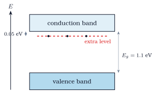
The figure shows the bands of doped silicon with an extra energy level.
Is this n-type or p-type silicon? Give the reason.
At \(300\) K the thermal energy is about \(kT = 0.026\) eV. Why are almost all the dopant atoms ionised at room temperature?
Why does thermal energy free very few electrons from the valence band?
Answer(i) n-type, donor level (ii) \(0.05\) eV \(\approx 2kT\) (iii) \(E_g \gg kT\)
Solution
n-type. The extra level lies just below the conduction band and holds the fifth electrons of donor atoms. Such an electron needs only \(0.05\) eV to enter the conduction band.
The donor electron needs \(0.05\) eV, only about twice \(kT\). Random thermal energy easily supplies this, so nearly every donor has given up its electron at \(300\) K.
A valence electron needs the full gap, \(1.1\) eV, more than \(40\) times \(kT\). Very few electrons ever collect this much thermal energy, so \(n_i\) stays small.
How did it go?
Q11
For the n-type silicon of Question 8, find the conductivity using \(\sigma \approx e n_e \mu_e\). How many times larger is it than the conductivity of pure silicon (Question 6)?
Answer\(216\) S/m; \(5 \times 10^{5}\)
Solution
\(\sigma = 1.6 \times 10^{-19} \times 10^{22} \times 0.135 = 216\) S/m. The hole term is negligible.
\(\dfrac{216}{4.4 \times 10^{-4}} \approx 5 \times 10^{5}\). One donor per five million atoms has raised the conductivity half a million times.
How did it go?
Q12
One silicon atom in a million is replaced by a phosphorus atom. Use the data of Questions 4 and 8.
Find the donor density \(N_D\) and hence \(n_e\).
Find \(n_h\).
Answer(i) \(5 \times 10^{22}\) m\(^{-3}\) (ii) \(4.5 \times 10^{9}\) m\(^{-3}\)
An n-type crystal has far more electrons than holes. Is the crystal negatively charged? Explain.
Answerno; fixed donor ions balance
Solution
No. Each free electron came from a phosphorus atom that is now a fixed positive ion. The extra electrons are balanced by the extra ionic charges, so the crystal as a whole is neutral. "n-type" describes the carriers, not the net charge.
How did it go?
The p-n junction
Q14
A p-type and an n-type piece are joined.
Which carriers diffuse across the junction, and in which directions?
What is left behind on each side, and what region does this form?
What stops the diffusion from continuing for ever?
Answer(i) \(e^-\) n\(\to\)p, holes p\(\to\)n (ii) fixed ions; depletion region (iii) the field
Solution
Electrons diffuse from the n side, where they are many, into the p side. Holes diffuse from the p side into the n side.
On the n side the donors left behind are fixed positive ions; on the p side the acceptors that gained electrons are fixed negative ions. This thin layer of fixed charge, with no free carriers, is the depletion region.
The fixed charges set up an electric field from n to p. This field opposes further diffusion and drives a drift current the other way. Diffusion and drift balance, and the junction settles with a potential barrier across it.
How did it go?
Q15
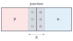
The figure shows an unbiased p-n junction. The region X contains fixed ions and no free carriers.
Name the region X. Why are the ions on the p side negative?
In which direction does the electric field in X point? Which way does it push an electron?
What is the potential barrier for silicon, roughly?
Answer(i) depletion region (ii) n to p; towards n (iii) \(0.7\) V
Solution
X is the depletion region. Electrons that diffused in from the n side have filled the holes of acceptor atoms there, leaving the acceptors as negative ions.
From the positive ions to the negative ions: from n to p. A field pushes an electron against its direction, so towards the n side, back where it came from.
About \(0.7\) V for silicon (\(0.3\) V for germanium).
How did it go?
Q16
A battery is connected across the junction. State what happens to the barrier height, the width of X and the current in each case.
The p side is connected to the positive terminal.
The n side is connected to the positive terminal.
Answer(i) lower, narrower, large (ii) higher, wider, tiny
Solution
Forward bias. The battery pushes holes and electrons towards the junction, the barrier is lowered by the applied voltage, and X becomes narrower. Once the applied voltage passes about \(0.7\) V, a large current flows.
Reverse bias. Carriers are pulled away from the junction, the barrier is raised, and X becomes wider. Only the few minority carriers cross, giving a current of microamperes that hardly depends on the voltage.
How did it go?
Q17
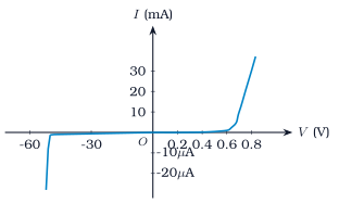
The figure shows the \(I\)-\(V\) characteristic of a silicon diode. Note the different scales on the two sides.
Read the knee voltage, below which the forward current is very small.
Read the forward current at \(0.8\) V.
Read the reverse current at \(-30\) V, and the voltage at which breakdown begins.
Answer(i) \(0.7\) V (ii) \(30\) mA (iii) \(1\ \mu\)A; \(50\) V
Solution
The current stays near zero until about \(0.7\) V and then rises steeply. The knee voltage is \(0.7\) V.
At \(0.8\) V the curve reads \(30\) mA.
At \(-30\) V the reverse current is about \(-1\ \mu\)A, thirty thousand times smaller than the forward current. Breakdown begins near \(-50\) V, where the current suddenly grows.
How did it go?
Q18
From the graph of Question 17, the current rises from \(20\) mA at \(0.75\) V to \(30\) mA at \(0.80\) V.
Find the dynamic resistance \(r = \frac{\Delta V}{\Delta I}\) in this range.
What is the dynamic resistance in reverse bias between \(-10\) V and \(-30\) V, roughly?
Answer(i) \(5\ \Omega\) (ii) \(\sim 10^{7}\ \Omega\)
Over \(20\) V the reverse current changes by perhaps \(1\ \mu\)A: \(r \approx \dfrac{20}{10^{-6}} = 2 \times 10^{7}\ \Omega\), of the order of \(10^{7}\ \Omega\). The diode is nearly an open switch.
How did it go?
Q19
A silicon diode is treated as a switch that drops \(0.7\) V when it conducts. It is in series with a \(430\ \Omega\) resistor and a \(5\) V battery, forward biased. Find the current.
Answer\(10\) mA
Solution
The diode takes \(0.7\) V, leaving \(5 - 0.7 = 4.3\) V across the resistor. \(I = \dfrac{4.3}{430} = 0.010\) A \(= 10\) mA.
How did it go?
Small situations
Q20
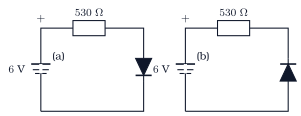
The figure shows two circuits with the same battery, resistor and silicon diode (forward drop \(0.7\) V).
In which circuit is the diode forward biased? How do you tell from the symbol?
Find the current and the voltage across the resistor in each circuit.
Find the voltage across the diode in each circuit.
Answer(i) (a) (ii) \(10\) mA, \(5.3\) V; \(0\), \(0\) (iii) \(0.7\) V; \(6\) V
Solution
Circuit (a). The triangle of the symbol points in the direction of easy (conventional) current flow. In (a) it points from the positive side of the battery round to the negative; in (b) it points against the battery.
(a): \(I = \dfrac{6 - 0.7}{530} = 10\) mA, and the resistor has \(10 \times 10^{-3} \times 530 = 5.3\) V across it. (b): no current, so \(0\) V across the resistor.
(a): \(0.7\) V, the forward drop. (b): the whole \(6\) V of the battery appears across the diode, since the resistor drops nothing.
How did it go?
Q21
The temperature of a diode rises. State, with a reason, what happens to
the reverse saturation current,
the barrier potential.
Answer(i) rises (ii) falls
Solution
It rises, roughly doubling for every \(10\) K. The reverse current is carried by minority carriers, and their number \(n_i^2/N\) grows rapidly with temperature.
It falls, by about \(2\) mV per kelvin. More carriers are present on both sides, so a smaller barrier is enough to balance the diffusion.
How did it go?
Q22
Photons of energy \(1.5\) eV and \(0.9\) eV fall in turn on silicon (\(E_g = 1.1\) eV) and on germanium (\(E_g = 0.7\) eV). In which of the four cases is an electron-hole pair created?
Answer\(1.5\) eV: both; \(0.9\) eV: Ge only
Solution
A pair is created only if the photon energy is at least \(E_g\).
\(1.5\) eV: above \(1.1\) eV and above \(0.7\) eV, so pairs in both Si and Ge. \(0.9\) eV: below \(1.1\) eV, no pair in Si; above \(0.7\) eV, a pair in Ge. Three of the four cases.
How did it go?
Q23
When the reverse bias on a junction is increased, the depletion region widens. Explain why, in terms of the carriers pulled away from the junction.
Answercarriers pulled away expose more ions
Solution
In reverse bias the positive terminal is on the n side and pulls electrons away from the junction. The negative terminal on the p side pulls holes away. More donor and acceptor ions are left uncovered on each side.
The layer of fixed charge with no free carriers therefore grows thicker, and the barrier voltage across it grows with the applied voltage.
How did it go?
Q24
In three or four sentences, explain why a p-n junction lets current pass easily in one direction and hardly at all in the other.
Answerforward lowers barrier; reverse raises it
Solution
The junction has a built-in barrier of about \(0.7\) V that stops the majority carriers crossing. A forward voltage cancels this barrier, so electrons from the n side and holes from the p side pour across and a large current flows.
A reverse voltage adds to the barrier and pulls the carriers away from the junction. Only the tiny number of minority carriers can cross, so the current is almost zero. The diode conducts one way only.