Questions on Diodes, Transistors and Logic Gates, the kind your examinations ask. Solve one on paper. Then tell the book how it went. The book believes you, and it uses your answer to plan your revision.
0%
Nothing marked yetMark honestly. Peek at the answer only after your own attempt.
Diode Circuits: Rectifiers, Clippers, Zener and Optoelectronics
24 questions · after Lesson 3, Diodes and Light: Photodiode, LED, Solar Cell
Rectifiers
Q1
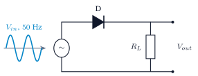
The figure shows a half-wave rectifier fed by a \(50\) Hz supply. Treat the diode as ideal.
During which half of the input cycle does D conduct? Sketch \(V_{out}\) against time.
What is the frequency of the output pulses?
Why is the output called direct current although it is not steady?
Answer(i) positive half (ii) \(50\) Hz (iii) one direction
Solution
D conducts when its anode (left) is positive, that is, during the positive half cycles. \(V_{out}\) is a series of positive half sine waves with gaps of zero between them.
One pulse per input cycle: \(50\) Hz.
The current through \(R_L\) always flows the same way, even though its size changes. Direct means one direction, not constant.
How did it go?
Q2
In a full-wave rectifier with a centre-tapped transformer, two diodes are used.
Which diode conducts during each half cycle, and why do both send current the same way through the load?
The input is \(50\) Hz. Find the frequency of the output.
Answer(i) one per half; both feed the load one way (ii) \(100\) Hz
Solution
The two ends of the secondary are always of opposite polarity with respect to the centre tap. In one half cycle the upper end is positive and \(D_1\) conducts; in the next the lower end is positive and \(D_2\) conducts. Both diodes feed the same end of the load, so the current through \(R_L\) is always in the same direction.
Both halves of each cycle give a pulse: \(2 \times 50 = 100\) Hz.
How did it go?
Q3
A bridge rectifier uses four diodes and no centre tap.
How many diodes conduct at any moment?
Give one advantage of the bridge over the centre-tap circuit.
Answer(i) \(2\) (ii) no centre tap, full voltage
Solution
Two, in series with the load, on opposite arms of the bridge. The other two are reverse biased.
The whole secondary voltage is used in each half cycle, so the peak output is twice that of a centre-tap circuit with the same transformer. No centre tap is needed. (Against this, two forward drops are lost instead of one.)
How did it go?
Q4
The supply to a rectifier is \(10\) V rms. Take \(\sqrt{2} = 1.41\) and a forward drop of \(0.7\) V per diode.
Find the peak input voltage.
Find the peak output voltage of a half-wave rectifier and of a bridge rectifier.
Answer(i) \(14.1\) V (ii) \(13.4\) V; \(12.7\) V
Solution
\(V_p = \sqrt{2} \times 10 = 14.1\) V.
Half-wave: one diode in the path, \(14.1 - 0.7 = 13.4\) V. Bridge: two diodes conduct in series, \(14.1 - 1.4 = 12.7\) V.
How did it go?
Q5
The average (dc) output of a half-wave rectifier is \(\frac{V_p}{\pi}\) and of a full-wave rectifier \(\frac{2V_p}{\pi}\). Find both for \(V_p = 14.1\) V. Why is the full-wave value twice as large?
Answer\(4.5\) V, \(9.0\) V; both halves used
Solution
Half-wave: \(\dfrac{14.1}{\pi} \approx 4.5\) V. Full-wave: \(\dfrac{2 \times 14.1}{\pi} \approx 9.0\) V.
The half-wave output is zero for half the time. The full-wave circuit fills those gaps with the inverted negative half cycles, so the average over a cycle doubles.
How did it go?
Q6
A capacitor \(C\) is connected across the load \(R_L\) of a rectifier.
Explain how the capacitor makes the output smoother.
For good smoothing \(R_L C\) must be much longer than the time between output peaks. Check this for \(R_L = 1\) k\(\Omega\), \(C = 100\ \mu\)F and a full-wave output from \(50\) Hz.
Answer(i) charges at peaks, discharges slowly (ii) \(0.1\) s \(\gg 10\) ms
Solution
Near each peak the diode conducts and charges the capacitor to nearly \(V_p\). When the input falls, the diode stops conducting and the capacitor discharges slowly through \(R_L\), holding the output up until the next peak. The dips are filled in.
\(R_L C = 10^{3} \times 10^{-4} = 0.1\) s. Full-wave peaks are \(10\) ms apart. \(0.1\) s is ten times longer, so the capacitor loses only a small part of its charge between peaks.
How did it go?
Q7
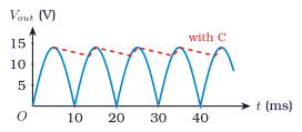
The figure shows the output of a full-wave rectifier without a capacitor (solid) and with one (dashed).
Read the peak voltage and the time between peaks. Find the output frequency and the input frequency.
Between what voltages does the filtered output ripple?
How could the ripple be made smaller?
Answer(i) \(14\) V, \(10\) ms; \(100\) Hz, \(50\) Hz (ii) \(12\) to \(14\) V (iii) larger \(C\) or \(R_L\)
Solution
Peak \(14\) V. Peaks at \(5\), \(15\), \(25\) ms: \(10\) ms apart, so the output frequency is \(100\) Hz. A full-wave rectifier doubles the frequency, so the input is \(50\) Hz.
The dashed line falls from \(14\) V to about \(12\) V before each new peak recharges the capacitor. The ripple is about \(2\) V.
Use a larger \(C\) or a larger \(R_L\) (a smaller load current), so that \(R_L C\) is longer and the capacitor discharges less between peaks.
How did it go?
Clippers and clampers
Q8
An ideal diode is connected in series with a load resistor. The input is a sine wave of peak \(10\) V. Sketch the output when the diode points towards the load, and when it is reversed.
Answerpositive half; negative half
Solution
Diode towards the load: it conducts for positive inputs only. Output: the positive half cycles, \(0\) to \(10\) V, with zero during the negative halves.
Diode reversed: it conducts for negative inputs only. Output: the negative half cycles, \(0\) to \(-10\) V, zero during the positive halves.
How did it go?
Q9
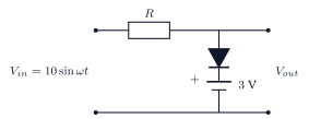
The figure shows a clipper with an ideal diode. The input is \(V_{in} = 10\sin\omega t\) volt.
For what input voltages does the diode conduct? What is \(V_{out}\) then?
What is \(V_{out}\) when the diode does not conduct?
Sketch \(V_{out}\) against time and mark the levels \(+3\) V and \(-10\) V.
Answer(i) \(V_{in} > 3\) V; \(3\) V (ii) \(V_{in}\) (iii) flat at \(+3\), down to \(-10\) V
Solution
The diode conducts when its anode is above its cathode, which sits at \(+3\) V. So it conducts when \(V_{in} > 3\) V. Then the output is held at \(3\) V; the excess voltage appears across \(R\).
When \(V_{in} < 3\) V the diode is off and no current flows through \(R\). \(V_{out} = V_{in}\).
The sine wave with its positive peaks cut flat at \(+3\) V. The negative half cycles are untouched and reach \(-10\) V.
How did it go?
Q10
The ideal diode in Question 9 is replaced by a silicon diode with a \(0.7\) V forward drop. At what voltage is the output now clipped?
Answer\(3.7\) V
Solution
The diode needs \(0.7\) V across it to conduct, so it turns on when \(V_{in} = 3 + 0.7 = 3.7\) V. The output is clipped at \(3.7\) V.
How did it go?
Q11
Two branches, each an ideal diode in series with a \(5\) V battery, are connected across the output. One clips the positive peaks and the other the negative peaks. The input is \(10\sin\omega t\) volt. Sketch \(V_{out}\) and state its maximum and minimum values.
Answer\(+5\) V, \(-5\) V
Solution
The upper branch conducts when \(V_{in} > 5\) V and holds the output at \(+5\) V. The lower branch conducts when \(V_{in} < -5\) V and holds it at \(-5\) V. In between, \(V_{out} = V_{in}\).
The output is the sine wave with both peaks cut flat: maximum \(+5\) V, minimum \(-5\) V.
How did it go?
Q12
A clamper uses a capacitor in series with the signal and an ideal diode across the output. The input is \(10\sin\omega t\) volt.
What does a clamper do to a waveform that a clipper does not?
A positive clamper shifts the whole wave up by \(10\) V. Between what values does the output swing?
Answer(i) shifts dc level, keeps shape (ii) \(0\) to \(20\) V
Solution
A clipper cuts off part of the wave and changes its shape. A clamper keeps the shape but shifts the whole wave up or down, adding a dc level.
The capacitor charges to \(10\) V on the first negative peak and then acts as a \(10\) V battery in series. The output is \(10\sin\omega t + 10\), swinging from \(0\) to \(+20\) V.
How did it go?
Zener diode
Q13
A Zener diode is used in reverse bias.
Sketch its \(I\)-\(V\) characteristic and mark the Zener voltage \(V_Z\).
Why is the voltage across it almost constant once it breaks down?
Why is a Zener diode heavily doped?
Answer(i) steep at \(-V_Z\) (ii) near-vertical curve (iii) thin layer, strong field
Solution
Forward: an ordinary diode curve rising after \(0.7\) V. Reverse: almost no current until \(-V_Z\), then the current rises very steeply while the voltage stays at \(-V_Z\). The reverse curve is nearly vertical at \(V_Z\).
The reverse curve is nearly vertical: a large change in current needs only a tiny change in voltage. So however much current flows (within limits), the voltage stays at \(V_Z\).
Heavy doping makes the depletion region very thin, so even a few volts give a very strong electric field across it. The field can then pull electrons out of the bonds (Zener breakdown) at a low, well-defined voltage.
How did it go?
Q14
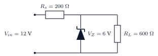
The figure shows a Zener regulator. The Zener is in breakdown.
Find the current through \(R_s\).
Find the load current and the Zener current.
Find the power dissipated in the Zener diode.
Answer(i) \(30\) mA (ii) \(10\) mA, \(20\) mA (iii) \(0.12\) W
Solution
The Zener holds its side at \(6\) V, so \(R_s\) has \(12 - 6 = 6\) V across it. \(I_s = \dfrac{6}{200} = 30\) mA.
\(I_L = \dfrac{6}{600} = 10\) mA. The rest goes through the Zener: \(I_Z = 30 - 10 = 20\) mA.
\(P_Z = V_Z I_Z = 6 \times 0.020 = 0.12\) W.
How did it go?
Q15
The input of the regulator in Question 14 rises to \(15\) V. Find the new currents through \(R_s\), \(R_L\) and the Zener. What happens to the output voltage?
The output stays at \(6\) V. The Zener absorbs the whole increase in current; that is how it regulates.
How did it go?
Q16
For the regulator of Question 14, the Zener needs at least \(5\) mA to stay in breakdown and can dissipate at most \(0.3\) W.
Find the least input voltage for which the output stays at \(6\) V.
Find the largest safe input voltage.
Answer(i) \(9\) V (ii) \(18\) V
Solution
With \(I_Z = 5\) mA and \(I_L = 10\) mA, \(I_s = 15\) mA. Then \(V_{in} = 6 + 200 \times 0.015 = 9\) V. Below this the Zener leaves breakdown and the output falls.
\(I_{Z,\max} = \dfrac{0.3}{6} = 50\) mA, so \(I_s = 60\) mA and \(V_{in} = 6 + 200 \times 0.060 = 18\) V.
How did it go?
Q17
The input is back at \(12\) V. The load is changed.
\(R_L = 300\ \Omega\). Find the load current and the Zener current.
\(R_L = 150\ \Omega\). Show that the Zener comes out of breakdown, and find the output voltage.
Answer(i) \(20\) mA, \(10\) mA (ii) \(5.1\) V
Solution
\(I_L = \dfrac{6}{300} = 20\) mA. \(I_s\) is still \(30\) mA, so \(I_Z = 10\) mA.
\(I_L\) would be \(\dfrac{6}{150} = 40\) mA, more than the \(30\) mA that \(R_s\) can supply at \(6\) V. The Zener current would be negative, which is impossible. The Zener switches off and \(R_s\), \(R_L\) form a plain divider: \(V_{out} = 12 \times \dfrac{150}{350} \approx 5.1\) V.
How did it go?
Q18
Compare Zener breakdown and avalanche breakdown. Cover the doping level, the depletion width, the mechanism, the voltage range and the change of \(V_Z\) with temperature.
Zener breakdown: heavy doping, a very thin depletion layer, a strong field that pulls electrons directly out of bonds (tunnelling). Occurs below about \(5\) V. \(V_Z\) falls slightly as temperature rises (negative coefficient).
Avalanche breakdown: lighter doping, a wider depletion layer. A minority carrier is accelerated by the field, knocks out more carriers, and the numbers multiply like an avalanche. Occurs above about \(6\) V. \(V_Z\) rises slightly with temperature (positive coefficient). Between \(5\) and \(6\) V both act, and the coefficient is nearly zero.
How did it go?
Optoelectronic devices
Q19
A light-emitting diode is forward biased. Take \(hc = 1240\) eV nm.
Where does the light come from?
An LED has band gap \(1.9\) eV. Find the wavelength and the colour of its light.
What band gap is needed for a blue LED at \(470\) nm?
Why is silicon not used to make LEDs?
Answer(i) recombination (ii) \(653\) nm, red (iii) \(2.6\) eV (iv) IR, heat
Solution
In forward bias electrons and holes are pushed into the junction and recombine. Each recombination releases the gap energy \(E_g\), and in a suitable material this energy leaves as a photon.
Silicon has \(E_g = 1.1\) eV, which would give infrared light (\(1130\) nm), not visible. Also, in silicon the recombination energy goes mostly into heat, not photons. Compounds such as GaAs and GaN are used instead.
How did it go?
Q20
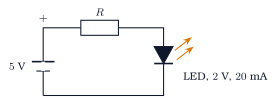
The LED in the figure drops \(2\) V and should carry \(20\) mA.
Find the value of the series resistor \(R\).
Find the power in \(R\) and in the LED.
What would happen without \(R\)?
Answer(i) \(150\ \Omega\) (ii) \(60\) mW, \(40\) mW (iii) LED burns out
Solution
The resistor takes \(5 - 2 = 3\) V at \(20\) mA: \(R = \dfrac{3}{0.020} = 150\ \Omega\).
The LED would have \(5\) V across it. Its forward current rises very steeply above \(2\) V, so a huge current would flow and burn it out at once. The resistor limits the current.
How did it go?
Q21
A photodiode is operated in reverse bias.
Why reverse and not forward bias?
What must be true of the photon energy for the diode to respond?
Find the longest wavelength a silicon photodiode (\(E_g = 1.1\) eV) can detect.
Answer(i) small dark current (ii) \(h\nu \ge E_g\) (iii) \(1130\) nm
Solution
In reverse bias the dark current is tiny, so the extra current made by light stands out and is proportional to the light intensity. In forward bias the large ordinary current would swamp the small photocurrent.
The photon energy must be at least the band gap, \(h\nu \ge E_g\), so that it can create an electron-hole pair.
\(\lambda_{\max} = \dfrac{1240}{1.1} \approx 1130\) nm, in the near infrared. All visible light is detected.
How did it go?
Q22
A photodiode absorbs \(10^{15}\) photons per second. Each creates one electron-hole pair, and \(80\%\) of the pairs reach the terminals. Take \(e = 1.6 \times 10^{-19}\) C. Find the photocurrent in microampere.
Answer\(128\ \mu\)A
Solution
Electrons collected per second \(= 0.8 \times 10^{15} = 8 \times 10^{14}\).
A solar cell is a p-n junction with no external bias.
Why does light falling on the junction produce a voltage?
A cell of area \(100\) cm\(^2\) receives sunlight of \(1000\) W/m\(^2\) and converts \(20\%\) into electricity. Find the electrical power.
Answer(i) field separates pairs (ii) \(2\) W
Solution
Photons create electron-hole pairs in and near the depletion region. The built-in field there sweeps electrons to the n side and holes to the p side. The separated charges make the p side positive and the n side negative: a voltage appears with no battery.
Area \(= 100\) cm\(^2 = 0.01\) m\(^2\). Power in \(= 1000 \times 0.01 = 10\) W. Power out \(= 0.2 \times 10 = 2\) W.
How did it go?
Q24
Make a table for the LED, the photodiode and the solar cell: the bias used, what goes in, and what comes out.
LED: forward bias; electrical energy in; light out. Turns current into photons.
Photodiode: reverse bias; light in; a current proportional to the light out. Used to detect and measure light.
Solar cell: no bias; light in; electrical power out. Turns photons into current and voltage, the reverse of the LED.
How did it go?
Logic Gates
24 questions · after Lesson 6, NAND, NOR and De Morgan
Basic gates
Q25
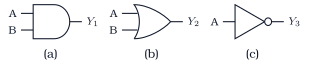
The figure shows three gate symbols.
Name each gate.
Write the Boolean expression for \(Y_1\), \(Y_2\) and \(Y_3\).
Answer(i) AND, OR, NOT (ii) \(A \cdot B\), \(A + B\), \(\bar{A}\)
Solution
(a) is the AND gate (flat back, round front). (b) is the OR gate (curved back, pointed front). (c) is the NOT gate (triangle with a small circle, the inversion bubble).
\(Y_1 = A \cdot B\), \(Y_2 = A + B\), \(Y_3 = \bar{A}\).
How did it go?
Q26
Write the truth table of the OR gate, the AND gate and the NOT gate.
AnswerOR \(0111\); AND \(0001\); NOT \(10\)
Solution
OR (\(Y = A + B\)): \(00 \to 0\), \(01 \to 1\), \(10 \to 1\), \(11 \to 1\). Output \(1\) if any input is \(1\).
AND (\(Y = A \cdot B\)): \(00 \to 0\), \(01 \to 0\), \(10 \to 0\), \(11 \to 1\). Output \(1\) only if all inputs are \(1\).
NOT (\(Y = \bar{A}\)): \(0 \to 1\), \(1 \to 0\).
How did it go?
Q27
Simplify each expression. Here \(\bar{A}\) means NOT \(A\).
(i) \(A + 0 = A\). (ii) \(A + 1 = 1\). (iii) \(A \cdot 0 = 0\). (iv) \(A \cdot 1 = A\). (v) \(A + A = A\). (vi) \(A \cdot \bar{A} = 0\): a thing and its opposite are never both true. (vii) \(A + \bar{A} = 1\): one of them is always true.
How did it go?
Q28
Find \(Y = A \cdot B + C\) for the inputs \((A, B, C) =\)
\((1, 0, 1)\),
\((1, 1, 0)\),
\((0, 0, 0)\).
Answer(i) \(1\) (ii) \(1\) (iii) \(0\)
Solution
\(1 \cdot 0 + 1 = 0 + 1 = 1\).
\(1 \cdot 1 + 0 = 1 + 0 = 1\).
\(0 \cdot 0 + 0 = 0\).
How did it go?
Q29
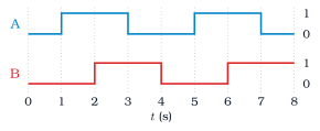
The figure shows two inputs A and B against time.
Between which times is \(Y = A \cdot B\) high? Draw the output.
Between which times is \(Y = A + B\) high?
How many pulses does each output show in \(8\) s?
Answer(i) \(2\) to \(3\), \(6\) to \(7\) s (ii) \(1\) to \(4\), \(5\) to \(8\) s (iii) \(2\), \(2\)
Solution
AND is high only when both are high. A is high \(1\) to \(3\) s and \(5\) to \(7\) s; B is high \(2\) to \(4\) s and \(6\) to \(8\) s. Both are high from \(2\) to \(3\) s and from \(6\) to \(7\) s. The output is two pulses of \(1\) s.
OR is high when either is high: from \(1\) to \(4\) s and from \(5\) to \(8\) s. Two pulses of \(3\) s, low only for \(0\) to \(1\) s and \(4\) to \(5\) s.
Two pulses each, but the AND pulses are short and the OR pulses long.
How did it go?
Q30
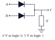
The figure shows a gate made from two diodes and a resistor.
A is at \(5\) V and B at \(0\) V. Which diode conducts, and what is \(Y\) (ignore the diode drop)?
Both inputs are at \(0\) V. What is \(Y\)?
Which gate is this? Write its truth table.
Answer(i) upper; \(5\) V (ii) \(0\) V (iii) OR
Solution
The upper diode has \(5\) V on its anode and conducts, pulling Y up to \(5\) V across \(R\). The lower diode has \(0\) V on its anode and \(5\) V on its cathode: reverse biased, off. \(Y = 5\) V, logic \(1\).
Neither diode conducts. No current flows in \(R\), so \(Y\) sits at \(0\) V through \(R\): logic \(0\).
Output \(1\) if A or B (or both) is \(1\): an OR gate. \(00 \to 0\), \(01 \to 1\), \(10 \to 1\), \(11 \to 1\).
How did it go?
Q31
A NOT gate can be made from a transistor with a resistor in its collector lead. Explain in a few sentences how a high input gives a low output and a low input gives a high output.
Answerhigh in: saturated, collector low; low in: off, high
Solution
The input goes to the base, the output is taken from the collector, and a resistor joins the collector to the supply.
Input high: base current flows, the transistor turns fully on (saturates), and the collector is pulled down almost to \(0\) V. Output low.
Input low: no base current, the transistor is off, no current flows in the collector resistor, and the collector sits at the supply voltage. Output high. The output is always the opposite of the input.
How did it go?
Universal gates
Q32
Draw the symbols of the NAND gate and the NOR gate. Write the Boolean expression and the truth table of each.
NAND: an AND symbol with a bubble on the output. \(Y = \overline{A \cdot B}\). Table: \(00 \to 1\), \(01 \to 1\), \(10 \to 1\), \(11 \to 0\).
NOR: an OR symbol with a bubble on the output. \(Y = \overline{A + B}\). Table: \(00 \to 1\), \(01 \to 0\), \(10 \to 0\), \(11 \to 0\).
How did it go?
Q33
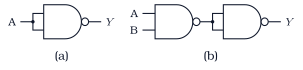
The figure shows two circuits built only from NAND gates.
In (a) both inputs of the NAND gate are joined. Write its truth table. Which gate is this?
In (b) a NAND is followed by the gate of (a). Which gate does the whole circuit make?
Answer(i) NOT (ii) AND
Solution
With both inputs equal to A: \(Y = \overline{A \cdot A} = \bar{A}\). Table: \(0 \to 1\), \(1 \to 0\). It is a NOT gate.
The first NAND gives \(\overline{A \cdot B}\). The second inverts it: \(\overline{\overline{A \cdot B}} = A \cdot B\). The whole circuit is an AND gate.
How did it go?
Q34
Draw an OR gate made only of NAND gates. Use three NAND gates. Prove your circuit works with Boolean algebra.
Answertwo NOTs, then NAND: \(\overline{\bar{A}\bar{B}} = A + B\)
Solution
Use two NAND gates as NOT gates (inputs joined) to make \(\bar{A}\) and \(\bar{B}\). Feed these into a third NAND: \(Y = \overline{\bar{A} \cdot \bar{B}}\).
By De Morgan, \(\overline{\bar{A} \cdot \bar{B}} = \bar{\bar{A}} + \bar{\bar{B}} = A + B\). The circuit is an OR gate.
How did it go?
Q35
Show how to make a NOT gate, an OR gate and an AND gate using only NOR gates. Say how many NOR gates each needs.
Answer\(1\), \(2\), \(3\) NOR gates
Solution
NOT: one NOR with its inputs joined, \(\overline{A + A} = \bar{A}\).
OR: a NOR followed by a NOR used as NOT, \(\overline{\overline{A + B}} = A + B\). Two gates.
AND: invert each input with a NOR-as-NOT, then NOR them: \(\overline{\bar{A} + \bar{B}} = A \cdot B\) by De Morgan. Three gates.
How did it go?
Q36
State De Morgan's two theorems. Verify \(\overline{A + B} = \bar{A} \cdot \bar{B}\) with a truth table.
Answer\(\overline{A+B} = \bar{A}\bar{B}\), \(\overline{AB} = \bar{A} + \bar{B}\); both \(1000\)
Solution
First theorem: \(\overline{A + B} = \bar{A} \cdot \bar{B}\). Second theorem: \(\overline{A \cdot B} = \bar{A} + \bar{B}\). To invert a whole expression, invert each term and swap \(+\) with \(\cdot\).
Check: \(00\): \(\overline{0} = 1\) and \(1 \cdot 1 = 1\). \(01\): \(\overline{1} = 0\) and \(1 \cdot 0 = 0\). \(10\): \(0\) and \(0 \cdot 1 = 0\). \(11\): \(0\) and \(0 \cdot 0 = 0\). The two columns agree in every row.
How did it go?
Q37
Why are NAND and NOR called universal gates?
AnswerAND, OR, NOT all from one type
Solution
Every logic function can be written with AND, OR and NOT. Questions 9 to 11 show that each of these three can be built from NAND gates alone, or from NOR gates alone. So any circuit at all can be built from one type of gate. That is why NAND and NOR are called universal.
Simplify each expression and name the single gate it equals.
\(Y = A + A \cdot B\)
\(Y = A \cdot B + A \cdot \bar{B}\)
\(Y = (A + B) \cdot \bar{A}\) when \(B = 1\)
Answer(i) \(A\) (ii) \(A\) (iii) \(\bar{A}\), NOT
Solution
\(A + A \cdot B = A(1 + B) = A \cdot 1 = A\). If A is \(1\) the output is \(1\) whatever B is; if A is \(0\) both terms are \(0\). No gate is needed; the output is just A.
\(A \cdot B + A \cdot \bar{B} = A(B + \bar{B}) = A \cdot 1 = A\). Again just A.
With \(B = 1\): \((A + 1) \cdot \bar{A} = 1 \cdot \bar{A} = \bar{A}\). A NOT gate.
How did it go?
Combinations
Q40
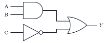
The figure shows a combination of three gates.
Write the Boolean expression for \(Y\).
Write the truth table. For how many of the eight input combinations is \(Y = 0\)?
Answer(i) \(A \cdot B + \bar{C}\) (ii) \(3\)
Solution
The AND gives \(A \cdot B\), the NOT gives \(\bar{C}\), and the OR combines them: \(Y = A \cdot B + \bar{C}\).
\(Y = 1\) whenever \(C = 0\) (four rows). When \(C = 1\), \(Y = A \cdot B\), which is \(1\) only for \(A = B = 1\). So \(Y = 0\) for \((0,0,1)\), \((0,1,1)\) and \((1,0,1)\): three of the eight rows.
How did it go?
Q41
How many rows does the truth table of a gate with \(n\) inputs have? Give the number for \(2\), \(3\) and \(4\) inputs.
Answer\(2^n\); \(4\), \(8\), \(16\)
Solution
Each input can be \(0\) or \(1\), so \(n\) inputs give \(2^n\) combinations. That is \(4\) rows for \(2\) inputs, \(8\) for \(3\) and \(16\) for \(4\).
How did it go?
Q42
A three-input AND gate and a three-input OR gate are given the same inputs.
For which inputs is the AND output \(1\)?
For which inputs is the OR output \(0\)?
For how many of the eight input combinations do the two gates agree?
Answer(i) \(111\) (ii) \(000\) (iii) \(2\)
Solution
Only for \(A = B = C = 1\): one row out of eight.
Only for \(A = B = C = 0\): one row out of eight.
They agree only for \(000\) (both \(0\)) and \(111\) (both \(1\)). For the other six rows OR gives \(1\) and AND gives \(0\). Two rows.
How did it go?
Q43
Use the waveforms of Question 5. Between which times is the output high for
a NAND gate,
a NOR gate?
Answer(i) \(0\) to \(2\), \(3\) to \(6\), \(7\) to \(8\) s (ii) \(0\) to \(1\), \(4\) to \(5\) s
Solution
NAND is the opposite of AND. AND was high \(2\) to \(3\) s and \(6\) to \(7\) s. NAND is high everywhere else: \(0\) to \(2\), \(3\) to \(6\) and \(7\) to \(8\) s.
NOR is the opposite of OR. OR was low only \(0\) to \(1\) s and \(4\) to \(5\) s, so NOR is high exactly there.
How did it go?
Q44
The XOR (exclusive OR) gate has \(Y = A \cdot \bar{B} + \bar{A} \cdot B\).
Write its truth table. In words, when is \(Y = 1\)?
Which basic gates, and how many of each, are needed to build it from the expression?
Answer(i) \(0110\), inputs differ (ii) \(2\) NOT, \(2\) AND, \(1\) OR
Solution
\(00 \to 0\), \(01 \to 1\), \(10 \to 1\), \(11 \to 0\). \(Y = 1\) when the inputs are different, and \(0\) when they are the same. Unlike OR, both inputs high gives \(0\).
Two NOT gates for \(\bar{A}\) and \(\bar{B}\), two AND gates for \(A \cdot \bar{B}\) and \(\bar{A} \cdot B\), and one OR gate to add them. Five gates.
How did it go?
Small situations
Q45
Two switches control a lamp. Switch closed means \(1\), lamp on means \(1\).
The switches are in series. Which gate does the circuit act as?
The switches are in parallel. Which gate now?
Answer(i) AND (ii) OR
Solution
In series the lamp lights only when both switches are closed: AND.
In parallel the lamp lights when either switch is closed: OR.
How did it go?
Q46
A car sounds a warning if the engine is running (\(E = 1\)) and the seat belt is not fastened (\(S = 0\)). Write the Boolean expression for the warning \(W\) and name the gates needed.
Answer\(W = E \cdot \bar{S}\); NOT, AND
Solution
The warning needs E true and S false: \(W = E \cdot \bar{S}\).
A NOT gate makes \(\bar{S}\) from the belt signal, and an AND gate combines it with E. Check: \(E = 1\), \(S = 0\) gives \(1 \cdot 1 = 1\); belt fastened, \(S = 1\), gives \(1 \cdot 0 = 0\).
How did it go?
Q47
Two one-bit numbers \(A\) and \(B\) are added. The sum bit is \(S\) and the carry bit is \(C\) (so \(1 + 1 = 10\) in binary).
Write the table of \(S\) and \(C\) for the four input pairs.
Which gate gives \(S\) and which gives \(C\)?
Answer(i) \(S\): \(0110\), \(C\): \(0001\) (ii) XOR; AND
The two sides agree in all four rows, so \(A + \bar{A} \cdot B = A + B\). In words: if A is already true, B does not matter; if A is false, the result is just B.